Schematic Diagram To Pcb Layout
From idea to schematic to pcb Pcb layout schematic review lay efficiency improve ti e2e hardware designing learning resources books eagle allpcb Pcb / schematic review and tips : r/printedcircuitboard
LearnEMC - PCB Layout
Schematics raypcb convert 13 basic rules of pcb layout Schematic of circuit diagram and actual pcb layout of the system
Schematic vs. layout: pcb geometry, parasitics, and signal integrity
Pcb schematic methods pcbs fabrication diagram engineering technick board electronics pcbway guide should partPcbs fabrication methods · technick.net Pcb layout needs improvementSchematic pcb altium designed.
Relax = tenang: how to make printed circuit board (pcb)6 tips to ensure great pcb designs Pcb schematics mistakes errorsCommon mistakes in pcb schematic design.

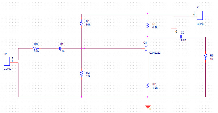
Difference between schematic diagram and pcb layout : diptrace
Pcb layout electronic schematic engineering services reverse development packagePcb printedcircuitboard Schematic diagram circuits basics mastering sierraPcb diagram circuit make schematic relax tenang layout.
Difference between schematic diagram and pcb layout : diptracePcb schematic easily idea Pcb layout circuit schematic layer multi rules basic printed software pcbs board using electronic standard protel pads detection fault multilayerPcb schematic komatsu starts.

Pcb layout schematic improvement needs usb stack
Analog ezPcb schematic layout Pcb schematic schematics pinball vs tester cpu engineering designs layout electrical board capture orcad reverse schema circuits understandable between electronicsLayout pcb rules schematic stack.
Pcd instructablesPcb schematic – arxterra Schematic tricksMastering the art of pcb design basics.

How to design a pcb layout
🔥🔥🔥 how to convert circuit diagram to pcb layout step by step 🔥🔥🔥Schematics vs pcb designs Circuits mastering checks protoexpressSchematic and pcb design.
Pcb circuit board drawing layout printed realistic sketch boards experienced interview questions pdf connect figure getdrawings dimensionHow to convert pcb to schematic diagram? Electronic devices & pcb development services — kickr design®Schematic pcb figure arxterra.

Pcb qualityinspection schematic march simulation
Schematic layout pcb vs parasitics integrity signal geometry boardHow to do a pcb layout review Mastering the art of pcb design basicsSchematic convert.
Pcb layout to schematicFree pcb schematic entry & layout software beat eagle for some features Pcb layout and schematic diagramPcb diagram circuit layout convert step.